When electronic assemblies have to meet the highest demands on temperature resistance and durability, classical soldering is limited and sintering shows its strengths.
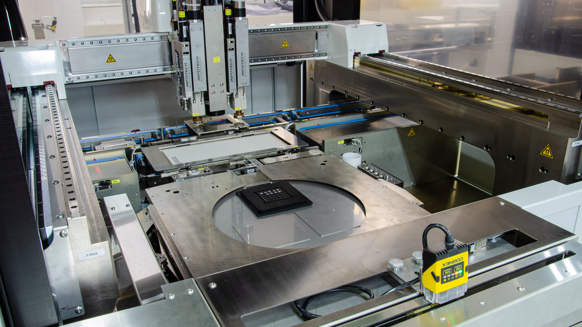
Interior view of a sinter bonder (Fig. INFOTECH AG)
Sinter bonding is a joining technology that is of great importance in electromobility. Power modules for these applications must meet the highest demands in terms of performance (temperature) and lifetime. The excellent physical properties of this connection between the power semiconductor and the substrate offer significant advantages over a conventional solder joint [1]. Silver as the metal in this sintered compound is preferably used because of the comparatively low sintering temperature and thus also reduced mechanical stresses between the bonding partners. The quantities needed to make a reliable sintered connection are pressure and temperature.
For small components (e.g., LEDs), specially equipped standard die bonders capable of carrying out the sinter bonding in one step are employed; the available bonding force meets the sintering requirements for the sintering process (about 10 to 20 MPa). The sintered layer itself can be applied to the semiconductor or the substrates by various methods (paste, DTF - Die Transfer Film, an Alpha Assembly Solutions, preform, etc.). For larger components, the semiconductor is fixed in a first step on the substrate (tacking), this also happens under temperature and pressure. The temperature must not reach the structure-changing temperature. In a second step, the parts are sintered with special tools (sintering press). These tools are usually designed so that all components on a substrate are sintered simultaneously.
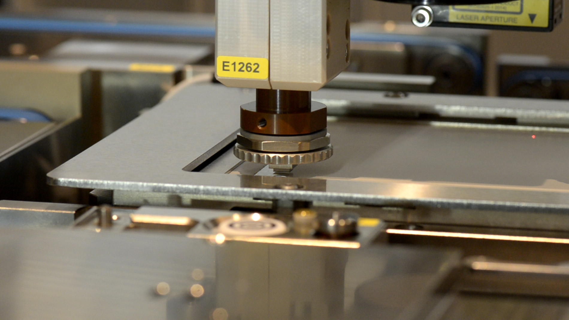
Sub-process – Dipping in DTF (Fig. INFOTECH AG)
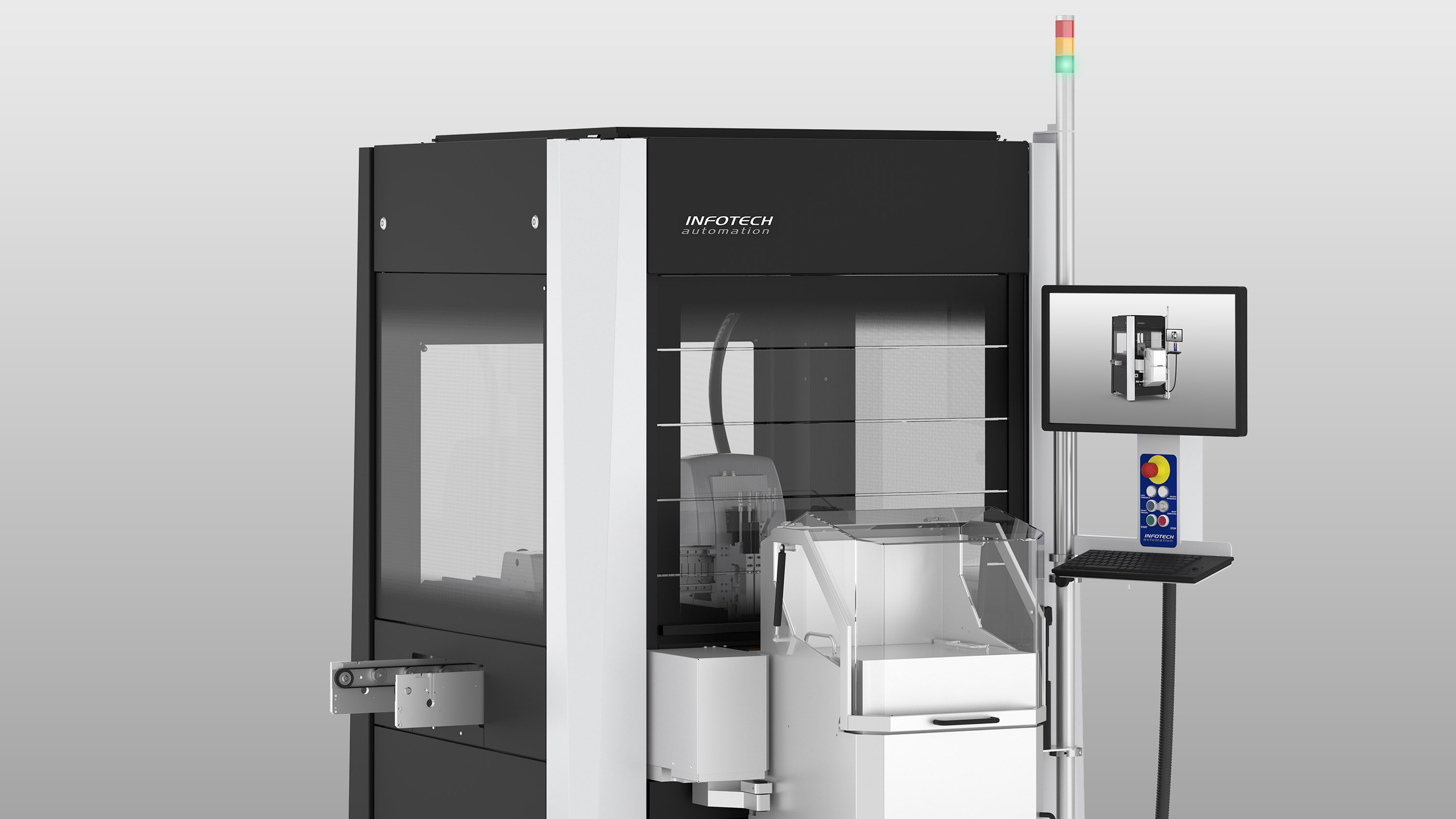
Infotech’s sinter bonder (Fig. 1) fulfills die attach requirements for power electronics exceeding standard die bonder capabilities. It is a highly flexible die bonder used for various production demands from laboratory up to series production. Out of the Infotech’s component matrix the system is equipped with sintering process specific components, i.e. heated bond head with high force capabilities, substrate pre-heater and heater station with integrated force measurement, DTF feeder (Fig. 2) and more. The system can operate as standalone system (batch processing) or as fully automated inline system as well. For larger die sizes, the sinter bonder is pre-sintering (tacking) the die onto the DBC substrate where a sinter press is performing the final sinter process. For smaller dies e.g. LED’s the sinter bonder can completely sinter the chip onto the substrate using two heated bond heads in sequence. Infotech’s specific solution for sinter bonding includes up to three heated bond heads with manual tool change, process heat profiles up to 300 °C, bond force capabilities up to 300 N (optional 500 N), heated substrate holder plate with manual tilt adjustment and integrated force sensing table, up to two standard assembly heads with interposer to transfer dice from cold to heated bond head, heated substrate surface up to 200 °C with integrated pre-heat station and support of DTF process from 4x4" waffle pack carrier size, Jedec carrier size or direct from wafer frames.
Literature
[1] Cyril Buttay, Amandine Masson, Jianfeng Li, Mark Johnson, Mihai Lazar, et al.. Die Attach of PowerDevices Using Silver Sintering - Bonding Process Optimization and Characterization. HiTEN 2011,Jul 2011, Oxford, United Kingdom. pp.1-7. hal-00672619
Power modules must meet the highest demands on performance and service life - there are many arguments in favor of sintering