The world's most successful panel-level packaging consortium will enter the next round after the successful completion of the two-year program and will again be open to new members and further topics. In December, the entire consortium will start again.
Mobile products in the consumer sector and autonomous driving are driving forces for the further development of electronic packaging. Fraunhofer IZM has been the ideal location for the last two years to develop basic processes for the new panel-level packaging with leading industrial companies from Europe, the USA, Japan, Korea and Taiwan and to realize the first demonstrators on these large organic substrates.
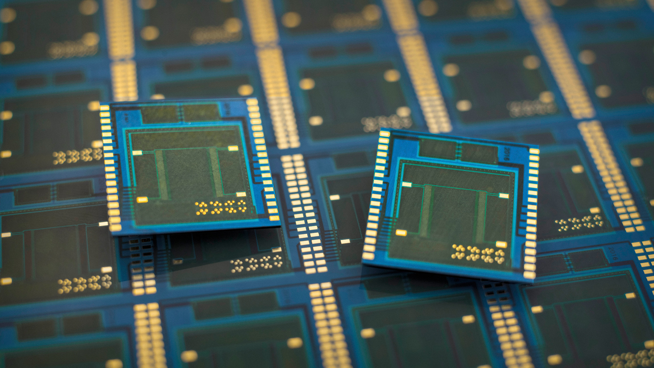
In the first round of the panel-level packaging consortium, Fraunhofer IZM and 17 industrial partners laid the foundations for industrially usable processes for the production of low-cost packages in panel format (18 x 24 inches). The result is very thin components that do without the usual substrate, but have excellent electrical properties and very low thermal resistance. Due to the short electrical connections, these packages are suitable for high frequency applications such as 5G and radar applications (e.g. autonomous driving). The focus of the two-year cooperation was the entire process chain of panel-level packaging: assembly, molding, rewiring, cost modeling and standardization.
"It is planned that the new consortium will start work in December 2019 and we are curious to see which companies will join us to reach the next level together."
The success prompted Fraunhofer IZM to plan a second consortium - the PLC 2.0. In contrast to the rather general goals in the first program, the partners are now concentrating on three specific approaches: Firstly, the further development and specification of technological development, especially with regard to the interfaces between the individual process steps. In the second stage, the wiring is to become ever finer and the limits of what is possible are to be reached. Due to further miniaturization at the chip level, a higher wiring density on the organic substrates is also absolutely necessary. Therefore, the PLC 2.0 consortium aims to achieve a wiring density of up to 2 μm line width and 2 μm distance. The aim is also to achieve the highest possible system reliability. For this reason, electromigration and copper diffusion will also be focal points of future research. An extended cost model rounds off the research project. In order to tackle these challenges, additional equipment installations were carried out at Fraunhofer IZM in the run-up to PLC 2.0. Thanks to the BMBF, some of the major investments were made within the Microelectronics Research Factory Germany. Due to the successful implementation of the workflow, there will only be one category of membership.
What has the first consortium achieved? 300,000 chips, 30,000 SMDs and 110 printed circuit boards within two years - the achievements speak for themselves: In the first year, the entire process chain from assembly through forming to device separation was established and optimized on a half-format panel (18 inches x 12 inches). For this purpose, test procedures and demonstrators were developed and initial reliability tests carried out. In the second year, the consortium then concentrated on modifying the design. Based on the results of the first year, the technology was scaled from half format to full format (18 x 24 inches) as well as vertical fasteners (VIE) and passive components were integrated. In addition to technical progress, a comprehensive cost model was developed that can be adapted to the application and material requirements. The standardization of panel sizes was discussed at various public events. Within the framework of SEMI, a standardization initiative was established with the participation of members of the Panel Level Packaging Consortium. In addition to Fraunhofer IZM, the following partners have contributed to the success of the PLP consortium: Ajinomoto Group, Amkor Technology, ASM Pacific Technology Ltd, Atotech Deutschland GmbH, Österreich Technologie & Systemtechnik AG, Brewer Science, Inc, Evatec AG, FUJIFILM Electronic Materials USA, Hitachi Chemical Company Ltd., Intel Corporation, Meltex Inc., Merck KGaA, Mitsui Chemicals Tohcello, Semsysco GmbH, ShinEtsu Chemical, SÜSS MicroTec SE and Unimicron Technology Corp.