
Microelectronic components are of crucial importance for the digital development of society and industry. The focus is on the fundamental megatrends digitization (Industry 4.0), E-Mobility, miniaturization and increasing environmental awareness. One of the current limiting factors for the rapid development of electronic components is joining technology. Conventional technologies have reached their performance limits and cannot fulfill the new performance requirements. NanoWired's technologies overcome these barriers and achieve the next performance boost in electronics.
"The new interconnection technologies not only meet future performance requirements of electronic components, but are already making performance boosts in electronics possible today," says Olav Birlem, CEO of NanoWired GmbH.
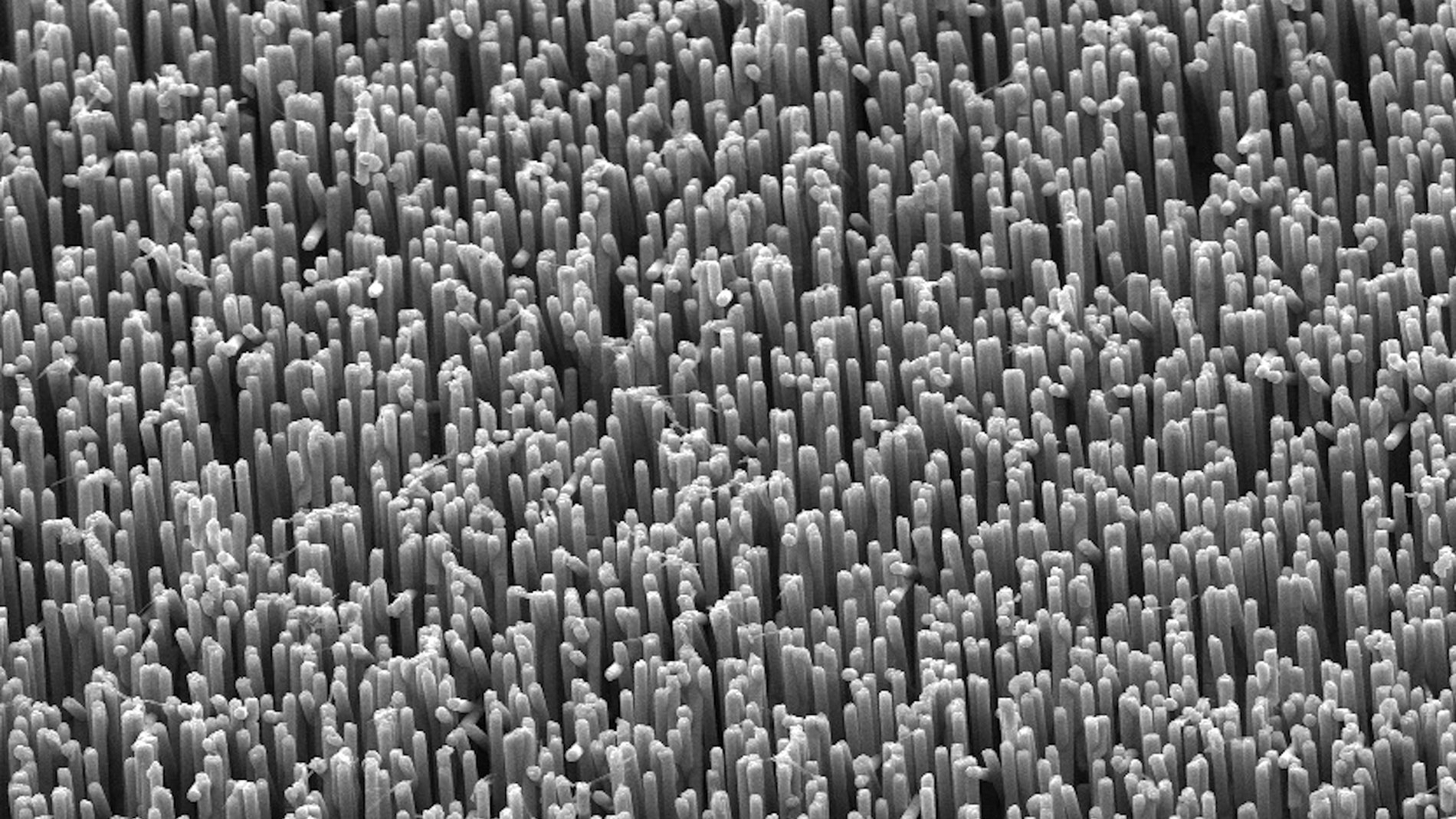
On the basis of more than 36 patent applications, four new, revolutionary assembly and interconnection technologies were developed against this background: NanoWiring, KlettWelding, KlettSintering, KlettGlueing. The core of these technologies is the joining of electrical components with Velcro fasteners consisting of nanometallic turf (Fig. 1). Any surfaces can be joined together in a metallic, thermally and mechanically stable manner. NanoWiring produces a metallic lawn on any surface (23 degree Celsius).
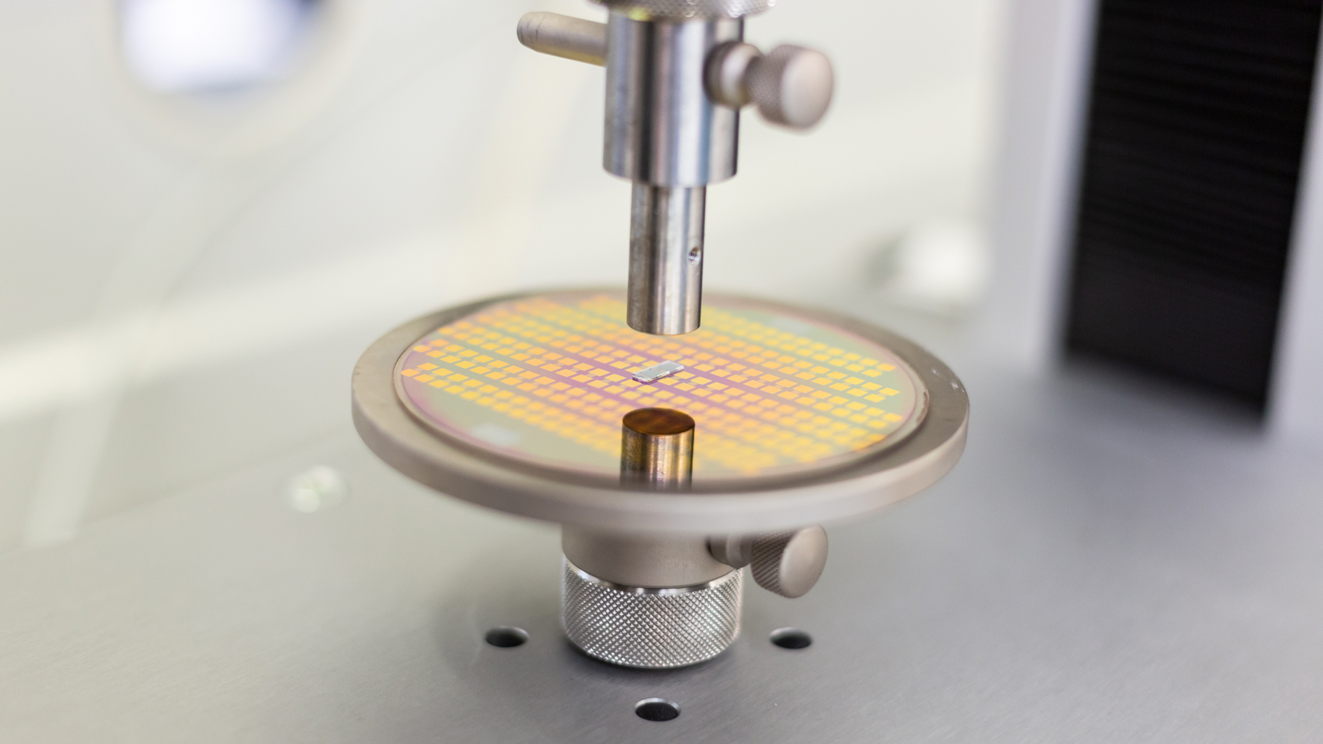
KlettWelding (Figure 2) realizes the connection of two substrates prepared with NanoWiring (23 degree Celsius). KlettSintering enables the connection with only one substrate prepared with NanoWiring (150 degree Celsius). KlettGlueing enables the contacting of fragile components with adhesive (23 degree Celsius). By using KlettWelding tape, even untreated substrates can be joined together.
The technologies are based on a pure copper, nickel, platinum, silver, zinc, tin or gold compound. They offer not only a higher thermal conductivity but also the required low contact resistance. In addition, the direct stacking of the components enables further geometric savings potential. In contrast to all other processes, KlettWelding and KlettSintering is a dry joining process. There are neither tensions due to shrinkage nor short circuits due to capillary connections. With KlettGlueing, conductive bonding can now be structured and at the same time carried out with a metallic dry process.
Contact

Related links
Tags
- Industry 4.0
- Miniaturization
- Digitalization