With the prototyping and reworking ever smaller electronic components, manual processing is increasingly reaching its limits. This requires the use of automated systems, where various aspects should be considered.
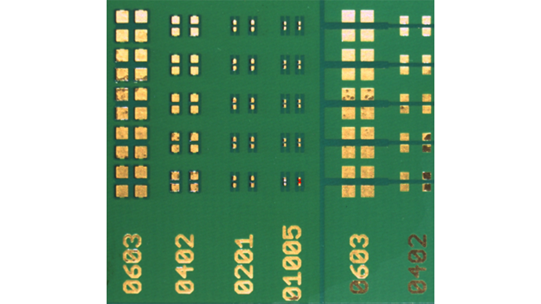
In the case of chip components, the package size has steadily decreased over the last few years. Small resistors and capacitors are still needed, even though chip designs and integration rates for integrated circuits are constantly improving. 0201 cases are state of the art in electronics production and smaller versions are entering the market. While production systems such as screen printers and pick-and-place machines can handle the small chips perfectly, rework and repair processes raise various questions. These include obstacles in the rework of 0201 and 01005 components or the question of which strategies and devices allow successful repair of these extremely small and sensitive components.
In the electronics industry, production quality is constantly improving. Higher automation, better equipment and standardized processes lead to better production results.
"Since zero-defect production is difficult to achieve, rework and repair processes must be introduced that meet the quality requirements of today's highly integrated and complex electronic products"
In addition to the "Big Board Rework Challenges", professional repair processes of the smallest chip components are one of the remaining challenges in PCB rework. Contrary to expectations, small chip components are not only used in compact applications such as smart phones, intelligent watches or hearing aids, but also on large boards.
Processing of chip components
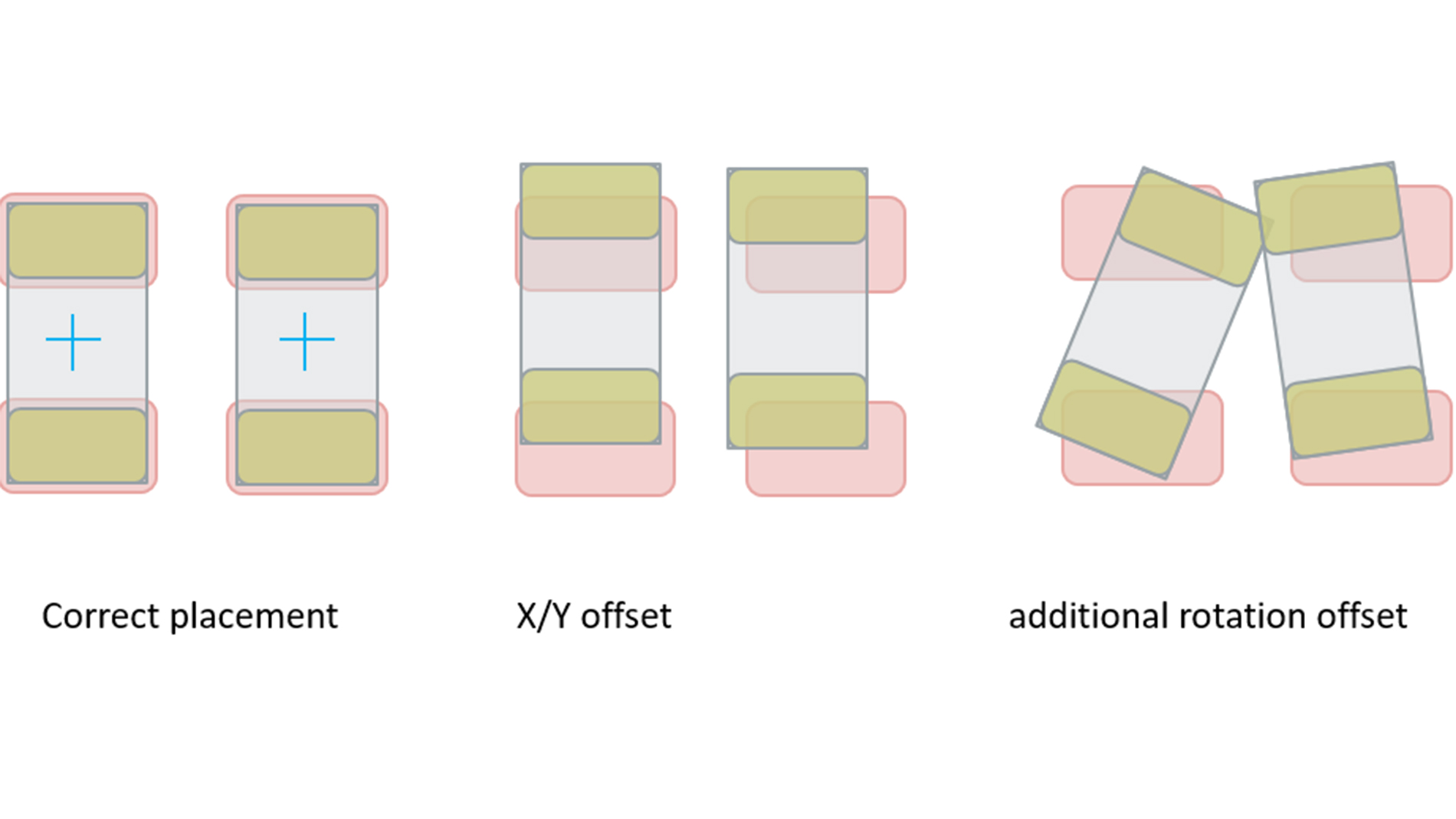
Fig. 1: Correct placement of the chip components (Fig.: ASM)
In production, the machining of chip components depends mainly on the tolerances of the components and the parameters of the placement machines (Fig. 1). In addition, the screen printing process is decisive for the subsequent soldering result. The machine parameters and the data sheet information of the components indicate the minimum possible placement distance. This gap finally defines the possible assembly density on the PCB. On the other hand, this assembly density can affect the ability to rework the components. If the gap is too narrow, it cannot be ruled out that repair work on one chip will affect the chips next to it.
Fig. 1: Correct placement of the chip components (Fig.: ASM)
Manual reworking of chip components
The processing of 0201 components in line production is standard today. Smaller versions are on the rise and all equipment manufacturers are concentrating on these requirements. At the same time, the situation for reworking is different. The following parameters can be an obstacle to the successful removal and installation of the tiny chips in a rework situation:
Dimensioning and handling of the components
Visualization and optical enlargement
Tools for heating processes
The pure dimensions of the small chip components (0201: 0.6 x 0.3 mm; 0.024 x 0.012 inch and 01005: 0.4 x 0.2 mm; 0.016 x 0.008 inch) are so small that manual handling requires patience and training. Unloading the component from a belt can already be difficult. It is important to have the correct handling tools (tweezers) to grip and release the chips securely. Carbon-based tweezer materials are an alternative to stainless steel. Adhesive effects sometimes hinder the operator in releasing the device, and of course the tips must not be contaminated with flux or solder paste. Experienced operators can handle 0201s without any optical magnification. However, working with 01005s requires optical enlargement. Most often, magnifying glasses or - even better - a stereomicroscope are used. The support of optical devices, such as cameras, is more than welcome for the pad preliminary inspection, the soldering process itself and the final evaluation of the soldering result.
As far as soldering tools are concerned, manual hot air tools are usually used. Hybrid systems (a combination of infrared heating and convection) have also proven to be suitable. Desoldering tweezers are also frequently used. Here, the soldering energy is transferred directly to the solder joint. This is a good way to remove the wrong or defective component.
Automated chip reworking
Due to these limitations in manual reworking, it is logical to demand more automated processes in the chip repair process. At the same time, rework is a task where it is not always possible to process several boards in a row. Therefore, the cost aspect and flexibility must remain in focus. A closer look at the individual steps of chip repair reveals the following four phases:
Removal of the components
Preparation of the pad
Select and place new component
Soldering the component
Desoldering an SMT component with a rework system has been an established process for many decades. For small chip components some aspects require additional attention:
Finding the correct position of the component on the PCB requires a high-resolution camera and a precise axis system. Otherwise it is impossible to lift the component during the desoldering process.
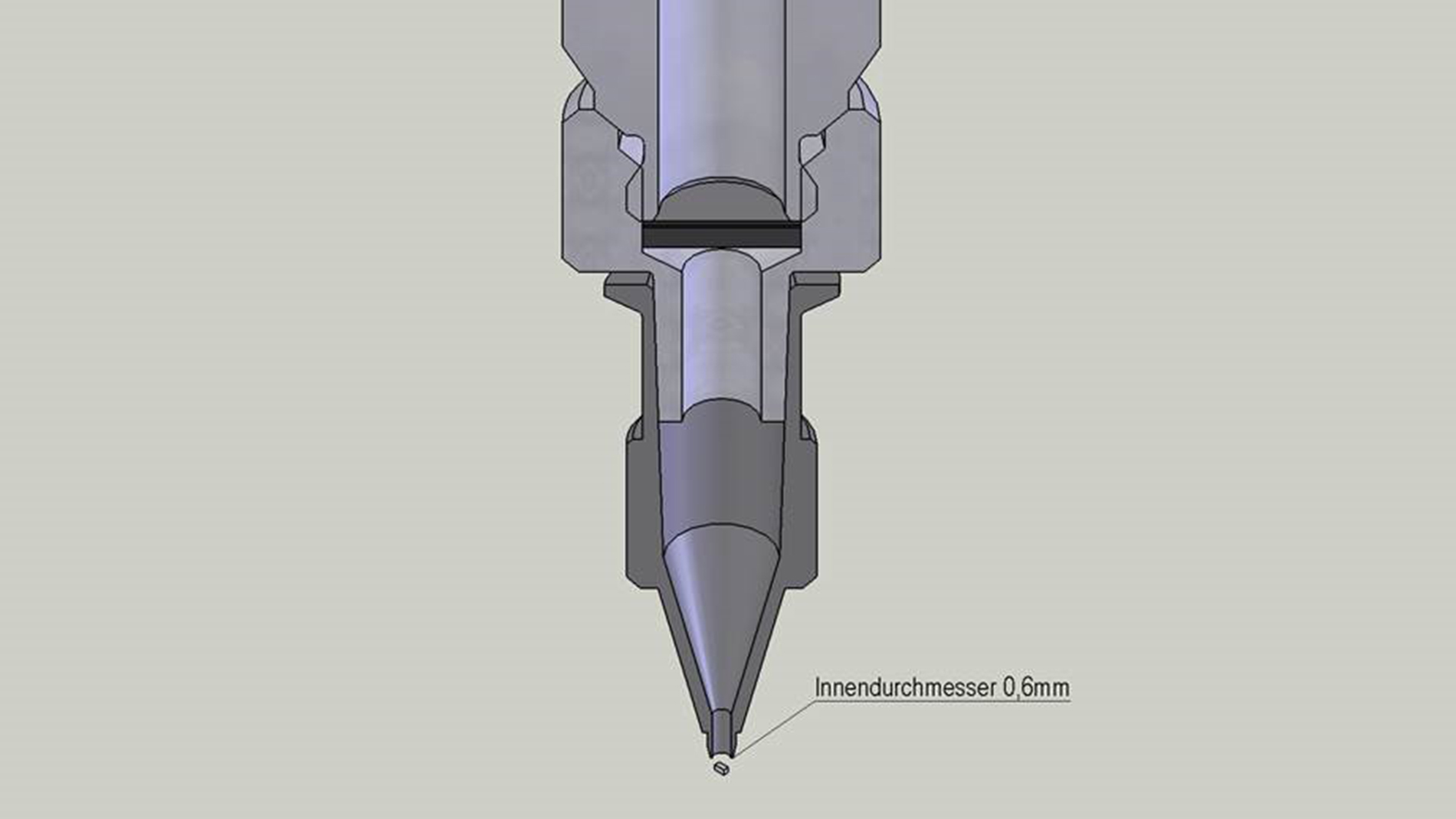
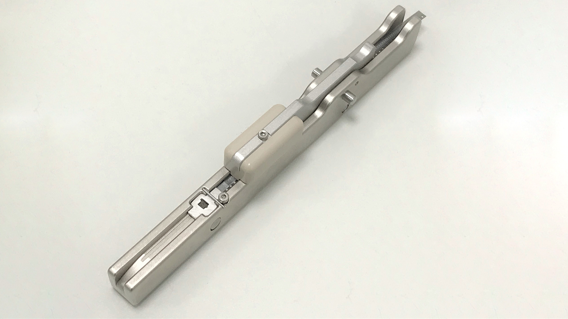
Fig.2: Nozzle design with integrated filter to collect chip components during removal (Fig.: Ersa GmbH)
The vacuum pick-up nozzle must overcome the adhesive forces of the liquid solder. Different nozzle designs are required to not pick up the chip but also to suck it off (Fig. 2).
The thermal process must be gentle and precise in order to reduce the thermal load on the assembly. Closed loop hybrid heating processes have proven that they meet these requirements. It is known that the reliability of the solder joint of adjacent components is not affected by an additional heating cycle, as is the case with other chips, but sensitive components in the vicinity must still be protected.
Fig.2: Nozzle design with integrated filter to collect chip components during removal (Fig.: Ersa GmbH)
If the component is removed from the PCB, the pads must be prepared for a new installation. During this phase various options are possible, which also depend on the initial production process, requirements and strategy of the user. Since the amount of solder in a 01005 connection is already very small, in many cases no separate rinse process will be necessary. The remaining amount of solder is very small after removing the components on the pad. The flux residues should also be negligible.
Flux removal or the addition of solder paste can be done using a dispensing device or with a manual or integrated dip transfer process. In this process a small needle is dipped into a paste depot and a defined amount of solder paste is transferred to the pads.
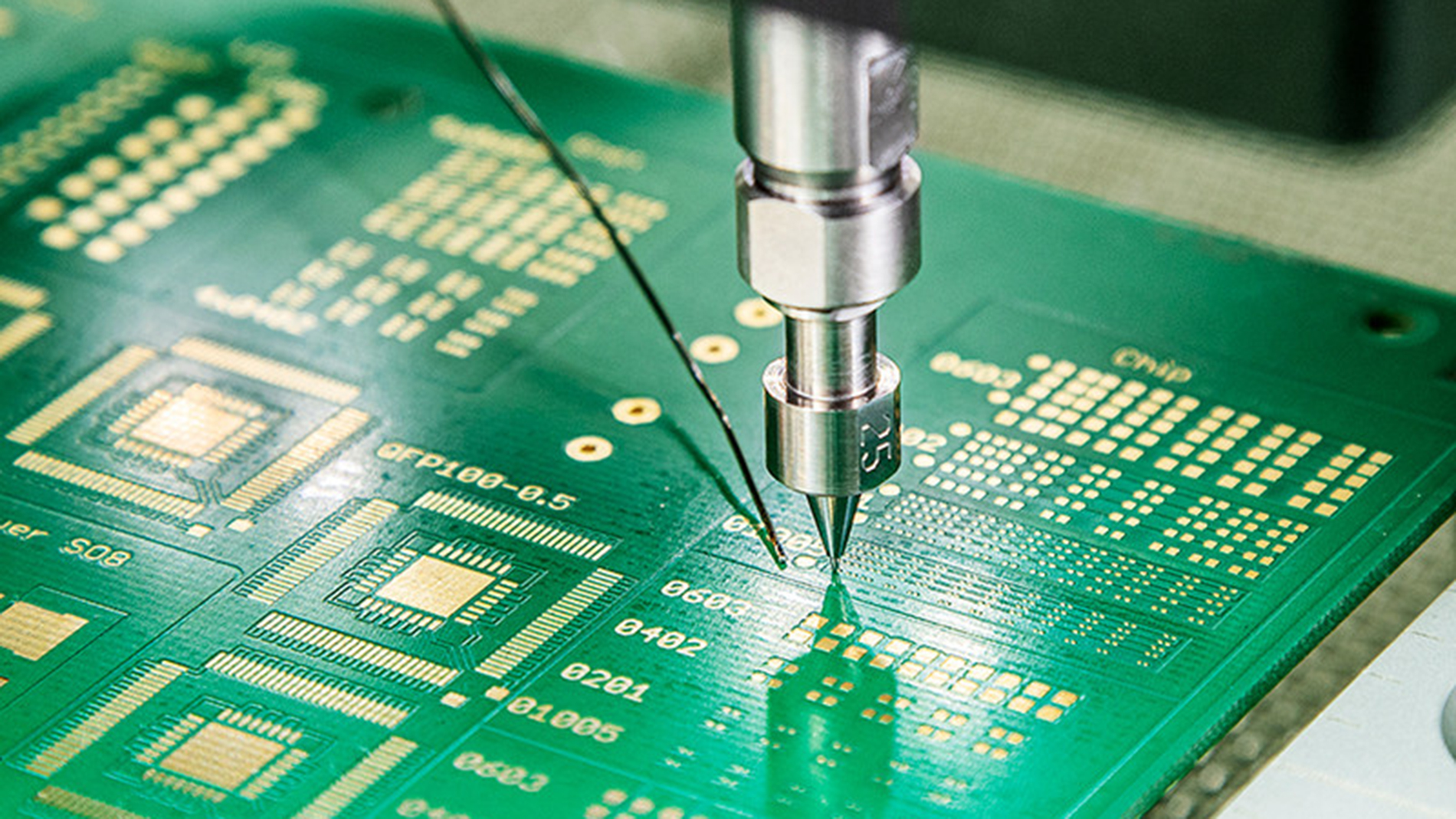
Fig. 3: Placement of a 01005 component (Fig.: Ersa GmbH)
The placement of 01005 components is probably the most difficult part of the entire repair process (Fig. 3). In a production line, chip shooters are often the most expensive systems. However, the available budget for rework is often limited. At the same time, precision and repeatability should also be at a "production-oriented" level. So when a 01005 chip has to be picked, the simple questions arise: How do you do that and how do you ensure that the right component is used? Manual picking from a box is not a good choice for several reasons, because:
Fig. 3: Placement of a 01005 component (Fig.: Ersa GmbH)
Is it safe to have only the right components in the box? Anyone who has ever removed screws from a magazine will know this problem.
Which is the right tool to grip the component and release it at the right place to pick it up?
Will the component be ideally aligned for pickup? In practice, these components behave like an egg placed on its tip.
Fig. 4: Strip feeding for installation on a rework system (Fig.: Ersa GmbH)
The only reasonable solution is to pick up the component directly from the belt (Fig. 4). Identification, orientation and transport provide the best basis. A tape feeder is required to present the device at a fixed position and enable the rework machine to find the device using image processing. It also ensures that the component is positioned in the correct orientation on the nozzle. Ideally, the tape is easy to load or the feeder consists of an interchangeable unit for different component tapes.
Fig. 4: Strip feeding for installation on a rework system (Fig.: Ersa GmbH)
Fig. 5: Test board with 01005 overlay and placements (Fig.: Ersa GmbH)
As far as chip removal is concerned, the nozzle design is also important in pick-and-place technology. Size and material must be suitable for picking up and releasing the device. Image processing is the final, but equally important integral component for automatic handling of the small chips. Component alignment and pins must be recognized. On the PCB the system has to find the appropriate pads and the best overlay (Fig. 5) has to be calculated. Later, the axis system moves the component to the target position and deposits it on the previously prepared solder paste or flux depot. The thermal requirements for chips are usually not an issue. Nevertheless, the heating processes should be controlled and gentle. As already mentioned, the lightweight components tend to move out of position when exposed to intensive air flow. A hybrid heating method seems to be the best method for soldering the components. Energy transfer by infrared radiation and a convective component are ideal. Further component-specific nozzles are not necessary and during the heating process the view of the very small solder joint is always available. A visual process observation with a reflow process camera device with high magnification and resolution is possible.
Fig. 5: Test board with 01005 overlay and placements (Fig.: Ersa GmbH)
Outlook
As 01005 and even smaller components are becoming more common in electronic assemblies, it is clear that the demand for prototyping and repair of such elements will increase. At the same time, process repeatability and process documentation will become increasingly important. No process without documentation is the goal. All OEMs and contract manufacturers are moving in the same direction, and system suppliers are called upon to offer integrated, highly automated rework solutions for all types of assemblies and components. It is foreseeable that further steps will be integrated into advanced rework system solutions: Component loss warnings as well as automated remount and re-soldering inspections as well as MES connectivity are just a few examples.