Functional ceramic wiring supports currently cost more than conventional circuit board solutions. However, if high thermal and electrical conductivity are required and/or harsh operating conditions prevail, the technology pays off – e.g. in energy and e-mobility applications.
Thus this technology is recommended e.g. for power electronics applications and those in which not only the price of the individual component but that of the overall system is taken into account. However, functional ceramic materials are still interesting in the context of another trend: microsystems will not only become significantly more complex, more robust and smaller in the future, but they will also increasingly interact directly with their environment through enhanced functionalities. This results in increasing demands on the development of cost-effective and reliable materials and manufacturing solutions for miniaturized assemblies. Fraunhofer IKTS solves these challenges by taking an integrated view of materials, processes and systems design.
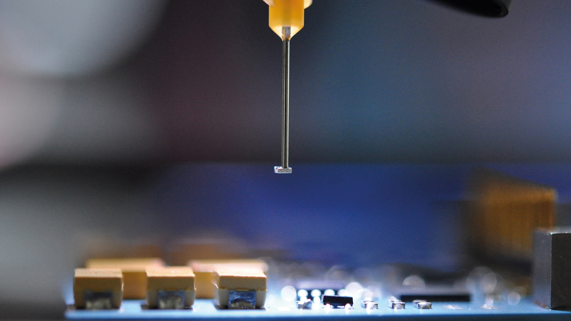
SMD assembly (Figure: Fraunhofer IKTS)
For today's and tomorrow's solutions, it is important to cover the entire spectrum of technical ceramics from basic research to application. The Fraunhofer Institute for Ceramic Technologies and Systems IKTS has more than 140 laboratories and technical facilities at its Dresden and Hermsdorf sites, covering almost 20,000 m² of floor space. The development of functional ceramic materials, miniaturized components and systems as well as ceramic-based sensors is the focus of the department "Hybrid Microsystems". The applications are in the fields of material development as well as assembly and connection technology (AVT) for electronics and power electronics, sensor technology and power engineering. The institute also has many years of expertise in the development of thick-film pastes.
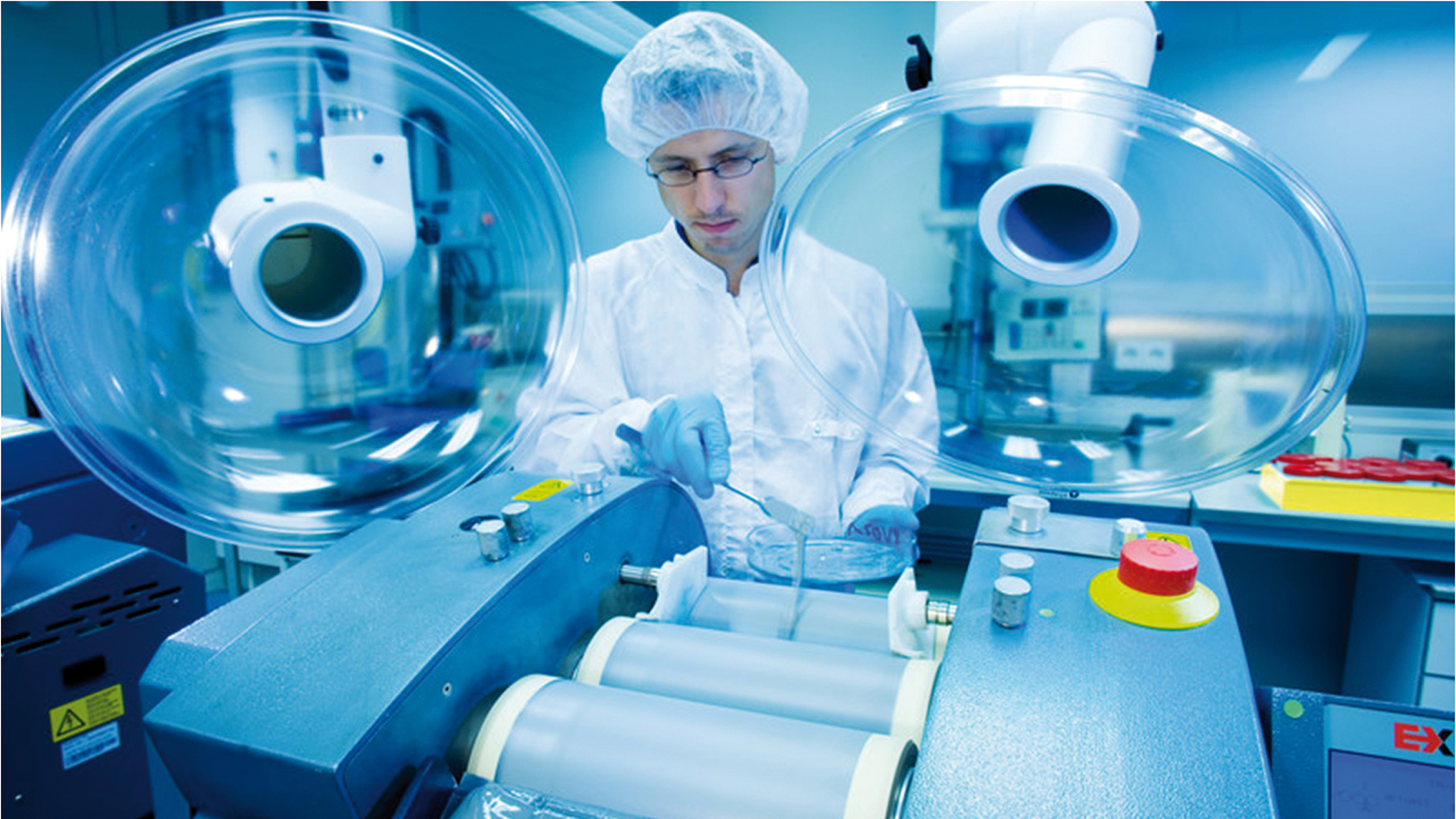
For the structured deposition of paste-based functional layers, other mask-based (stencil and engraving printing) and digital printing processes (aerosol and inkjet printing) can be used in addition to classical screen printing technology to meet application requirements. These can be used on flat as well as on tubular substrates. Currently, ceramic hybrid substrates are being developed and implemented in both standard thick-film and multilayer technology (LTCC and HTCC). A broad portfolio of typical contacting technologies (soldering, wire bonding, microwelding as well as assembly and contact bonding) is available for the instalation of complete assemblies on a laboratory scale and their system integration (Fig. 1). The necessary analysis technology (e.g. microstructure analysis/phase inventory, adhesion and shear strength) is used to characterize the contacts. This range is extended by analyses using both non-destructive and analytical testing. A wide range of possibilities is available for ageing tests. For the implementation of projects, the technological experience as well as the extensive preparatory work of the IKTS in the field of special electrical measurement methods are used. These include ESD measurements, but also the characterization of electrical properties of printed functional layers such as short-time overload (STOL) or current carrying capacity.
"Modern electronic solutions based on functional ceramic materials require a holistic approach. On this basis, the cost differences to printed circuit board solutions then – at increased requirements – become less and less significant."